- 您现在的位置:买卖IC网 > Sheet目录1992 > DAC8426EPZ (Analog Devices Inc)IC DAC 8BIT QUAD 10VREF 20PDIP
DAC8426
–8–
REV. C
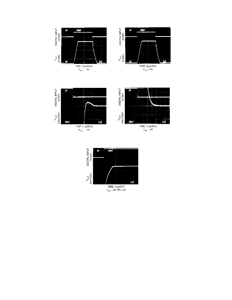
a) Large Signal
b) Settling Time Response (Negative Transition)
c) Settling Time Response (Positive Transition)
Figure 3. Dynamic Response
The outputs can withstand an indefinite short-circuit to AGND
to typically 50 mA. The output may also be shorted to any volt-
age between VDD and VSS; however, care must be taken to not
exceed the device maximum power dissipation.
The amplifier’s emitter follower output stage consists of an in-
trinsic NPN bipolar transistor with a 400
A NMOS pull-down
current-source load connected to VSS. This circuit configuration
shown in Figure 4 enables the output amplifier to develop out-
put voltages very close to AGND. Only the negative supply of the
four output buffer amplifiers are connected to VSS. Operating
the DAC8426 from dual supplies (VDD = +15 V and VSS = –5 V)
improves negative going output settling time near zero volts.
When operating single supply (VDD = +15 V and VSS = 0 V) the
output sink current decreases as the output approaches zero
voltage. Within 200 mV of AGND (single-supply operation) the
internal sinking capability appears resistive at a value of approxi-
mately 1200
. The buffer amplifier output current and voltage
characteristics are plotted in Figure 5.
Test Conditions, All Photos:
VDD = +15 V
CREFOUT = 10 F
RL = 2 k
Digital Input Sequence 0, 255, 0
发布紧急采购,3分钟左右您将得到回复。
相关PDF资料
DAC8531IDRBTG4
IC D/A CONV LP 16-BIT 8-SON
DAC8562FP
IC DAC 12BIT PARALLEL 5V 20-DIP
DS1004Z-5+T
IC DELAY LINE 5TAP 25NS 8-SOIC
DS1005-125+
IC DELAY LINE 5TAP 125NS 14-DIP
DS1007S-2+T&R
IC DELAY LINE 4NS 16-SOIC
DS1010S-50+T&R
IC DELAY LINE 10TAP 16-SOIC
DS1013S-25+T&R
IC DELAY LINE 25NS 16-SOIC
DS1020S-50+T
IC DELAY LINE 256TAP 16-SOIC
相关代理商/技术参数
DAC8426ER
制造商:AD 制造商全称:Analog Devices 功能描述:Quad 8-Bit Voltage Out CMOS DAC Complete with Internal 10 V Reference
DAC8426FP
功能描述:IC DAC 8BIT QUAD 10VREF 20-DIP RoHS:否 类别:集成电路 (IC) >> 数据采集 - 数模转换器 系列:- 产品培训模块:Lead (SnPb) Finish for COTS
Obsolescence Mitigation Program 标准包装:1,000 系列:- 设置时间:1µs 位数:8 数据接口:串行 转换器数目:8 电压电源:双 ± 功率耗散(最大):941mW 工作温度:0°C ~ 70°C 安装类型:表面贴装 封装/外壳:24-SOIC(0.295",7.50mm 宽) 供应商设备封装:24-SOIC W 包装:带卷 (TR) 输出数目和类型:8 电压,单极 采样率(每秒):*
DAC8426FPZ
功能描述:IC DAC 8BIT QUAD 10VREF 20DIP RoHS:是 类别:集成电路 (IC) >> 数据采集 - 数模转换器 系列:- 标准包装:1 系列:- 设置时间:4.5µs 位数:12 数据接口:串行,SPI? 转换器数目:1 电压电源:单电源 功率耗散(最大):- 工作温度:-40°C ~ 125°C 安装类型:表面贴装 封装/外壳:8-SOIC(0.154",3.90mm 宽) 供应商设备封装:8-SOICN 包装:剪切带 (CT) 输出数目和类型:1 电压,单极;1 电压,双极 采样率(每秒):* 其它名称:MCP4921T-E/SNCTMCP4921T-E/SNRCTMCP4921T-E/SNRCT-ND
DAC8426FR
制造商:Rochester Electronics LLC 功能描述:COMPLETE QUAD CMOS 8-BIT - Bulk 制造商:Analog Devices 功能描述:
DAC8426FS
功能描述:IC DAC 8BIT QUAD W/V-REF 20-SOIC RoHS:否 类别:集成电路 (IC) >> 数据采集 - 数模转换器 系列:- 产品培训模块:Lead (SnPb) Finish for COTS
Obsolescence Mitigation Program 标准包装:1,000 系列:- 设置时间:1µs 位数:8 数据接口:串行 转换器数目:8 电压电源:双 ± 功率耗散(最大):941mW 工作温度:0°C ~ 70°C 安装类型:表面贴装 封装/外壳:24-SOIC(0.295",7.50mm 宽) 供应商设备封装:24-SOIC W 包装:带卷 (TR) 输出数目和类型:8 电压,单极 采样率(每秒):*
DAC8426FSZ
功能描述:IC DAC 8BIT QUAD W/V-REF 20SOIC RoHS:是 类别:集成电路 (IC) >> 数据采集 - 数模转换器 系列:- 标准包装:1 系列:- 设置时间:4.5µs 位数:12 数据接口:串行,SPI? 转换器数目:1 电压电源:单电源 功率耗散(最大):- 工作温度:-40°C ~ 125°C 安装类型:表面贴装 封装/外壳:8-SOIC(0.154",3.90mm 宽) 供应商设备封装:8-SOICN 包装:剪切带 (CT) 输出数目和类型:1 电压,单极;1 电压,双极 采样率(每秒):* 其它名称:MCP4921T-E/SNCTMCP4921T-E/SNRCTMCP4921T-E/SNRCT-ND
DAC8426FSZ-REEL
功能描述:IC DAC 8BIT QUAD 10VREF 20SOIC RoHS:是 类别:集成电路 (IC) >> 数据采集 - 数模转换器 系列:- 标准包装:2,400 系列:- 设置时间:- 位数:18 数据接口:串行 转换器数目:3 电压电源:模拟和数字 功率耗散(最大):- 工作温度:-40°C ~ 85°C 安装类型:表面贴装 封装/外壳:36-TFBGA 供应商设备封装:36-TFBGA 包装:带卷 (TR) 输出数目和类型:* 采样率(每秒):*
DAC8501
制造商:BB 制造商全称:BB 功能描述:Low-Power, Rail-to-Rail Output, 16-Bit Serial Input DIGITAL-TO-ANALOG CONVERTER